Page 48 - Market Analysis Report of Optical Communications Field in China & Global market 2021
P. 48
͐ ͕ ͖ ͛ ͎
          WSS, up to 8 line directions, 13 local CDC modules are   However, this solution is a true monolithic integrated solution
          configured, up to 208 waves of up-drop are supported.   with great potential.
          At present, the more mature CDC technical solution in the   The most potential application of silicon photonics technology in
          industry is the Multi-channel Broadcasting Function Optical   the field of optical communications is photoelectric collaborative
          Switch (MCS). MCS is based on optical switches, couplers and   packaging (CPO), which is the mainstream solution for next-
          optical amplifier arrays. A large number of active devices will   generation on-board optical interconnection. Due to the limitations
          affect the reliability of the system. Therefore, the industry is   of material characteristics, signal integrity and integration, after
                                                                  the transmission rate reaches 800G or 1.6T, pluggable optical
          generally more optimistic about the NxM WSS solution, which is   modules will reach the technical bottleneck. CPO will be ahead of
          based on optical switches and WSS arrays, Lower insertion loss   traditional pluggable optical devices and on-board optical devices
          for up-drop, through reasonable power configuration, intermediate   in terms of cost and benefit. Its future application prospects in
          amplifiers can be omitted, higher up-drop dimensions can be   edge computing, metropolitan area networks, high-performance
          supported, the impact on transmission performance is smaller,   computing and sensors Very broad.
          and the reliability and integration are higher.
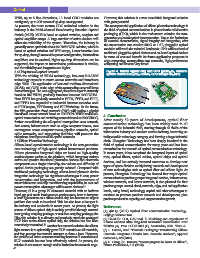
          3.4 Ubiquitous all-optical network                       Figure 4. Silicon optical chip and CPO packaging scheme
                                                                   (picture source: Hengtong Rockley CPO sample diagram)
          With the sinking of WDM technology, low-cost ROADM
          technology expands to metro access networks and introduces
          edge WSS. The application of low-and medium-dimensional
          (4D/9D, etc.) WSS at the edge of the metropolitan area will have
          cost advantages. The core aggregated, the access layer is currently
          based on 10G WDM, gradually introduce low-cost 100G WDM.
          Now FTTH has gradually extended to FTTR, FTTD, and FTTT,
          and FTTO has expanded to industrial Internet scenarios such
          as FTTCampus, FTTFactory, and FTTWorkshop. In the future,
          the fifth-generation fixed network (F5G) will realize a gigabit
          broadband access network based on 10G PON+WIFI6 and an all-  4. Conclusion
          optical transmission and switching network based on 200G/400G,   After nearly 50 years of development, optical fiber
          further consolidating the all-optical metropolitan area network,   communication technology has been widely used in all
          data center, Infrastructure such as edge computer rooms, core   aspects of the industrial field, running through all fields of the
          convergence access computer rooms, pipeline networks, optical
          cable networks, and supporting facilities will promote the   information industry and modern service industry, becoming an
          ubiquitous development of all-optical networks.         indispensable technology category, and forming a huge industrial
          3.5 Silicon Photonics Technology                        chain. Zhongtian Technology has been deeply involved in the
          Silicon-based optoelectronics technology is the next-generation   field of optical communication for many years and has been
          core technology of high-speed optical interconnect products.   committed to the research of optical communication technology.
          Silicon photonics integrated chips are based on high-quality   In recent years, it has completed the integrated layout of optical
          semiconductor wafers as the platform, which integrates various   rods, optical fibers, optical cables, optical chips and optical
          active and passive functional photonics devices and electronic   devices, and has actively invested resources to develop new
          components on a single microchip, the volume and difficulty of   types of space division multiplexing research and development
          optical device packaging are greatly reduced. Compared with   of new technologies such as optical fiber and silicon light. At
          traditional packaging technology, silicon-based photonic device   present, Zhongtian Technology has formed four major optical
          integration technology has significant advantages in cost, power   communication product groups: integrated service, infrastructure,
          consumption and integration, and with the improvement of
          transmission rate and chip manufacturing capabilities, its cost and   wireless network, and bearer network, It also planned the four
                                                     [3]
          power consumption advantages will be more obvious  .    product groups around cloud, network, edge, end and application
          However, Si is a group IV elemental material with an indirect   levels, using brand, technology, capital and other advantages to
          band gap and weak luminescence performance, how to integrate   continue to promote product research and development, plan
          a laser light source on a silicon-based chip has become an urgent   product production capacity, and support market growth.
          problem that needs to be solved. This has also been a hot spot in
          the industry and academia in recent years. At present, the light   References
          source of silicon optical chip is mainly provided through external   [1] Qiu Qi (2011) Optical fiber communication technology.
          laser grating coupling package or end-face coupling package; the   Beijing: Science Press
          Flip-chip solution is to directly and passively attach the packaged   [2] CLAUSE C B, CAVRAK S. Modeling and experiment of
          III-V laser to the silicon optical chip, the solution has also been   Raman assisted ultra long-haul terrestrial transmission over
                             [4]
          extensively researched . Another hot research solution for silicon   7500km [A]. Proc. ECOC 2001 [C]. Amsterdam, 2001. WeF1-2.
          light sources is to epitaxially grow III-V materials on Si materials,   [3] L. Carroll, et.al. "Photonic Packaging: Transforming Silicon
          and then process the material structure to form a laser. However,   Photonic Integrated Circuits into Photonic Devices", Applied
          the problem of lattice constant matching between Si materials and   Sciences 6, 426(2016)
          III-V materials has not been effectively solved. At present, the   [4] D. Liang, J.E. Bowers, "Recent progress in lasers on silicon",
          solution is not mature enough and is limited to the research stage.   Nature Photonics 4, 511 (2010)
         46

